Title: MOSAIC: Breaking the Optics versus Copper Trade-off with a Wide-and-Slow Architecture and MicroLEDs
Authors: Kaoutar Benyahya, Ariel Gomez Diaz, Junyi Liu, Vassily Lyutsarev, Marianna Pantouvaki, Kai Shi, Shawn Yohanes Siew, Hitesh Ballani, Thomas Burridge, Daniel Cletheroe, Thomas Karagiannis, Brian Robertson, Ant Rowstron, Mengyang Yang (Microsoft Research); Arash Behziz, Jamie Gaudette (Microsoft Azure); Paolo Costa (Microsoft Research)
Scribe: Mingyuan Song (Xiamen University)
Introduction: The Data Center Interconnect Stalemate

The Core Problem: A Trilemma of Reach, Power, and Reliability
Modern data centers, driven by the insatiable demands of cloud computing and artificial intelligence, are built upon a network fabric constrained by a fundamental compromise. Operators must navigate a trilemma when selecting interconnect technologies, choosing between reach, power, and reliability—a choice where optimizing one often degrades the others. The two incumbent technologies, copper and fiber optics, represent opposite ends of this trade-off. Electrical copper links are celebrated for their high reliability and power efficiency, but their reach is severely limited to less than 2 meters, confining their use to intra-rack connectivity. Conversely, active optical cables (AOCs) provide the reach necessary to span tens of meters between racks, but this comes at the cost of significantly higher power consumption and failure rates up to 100 times worse than their copper counterparts.
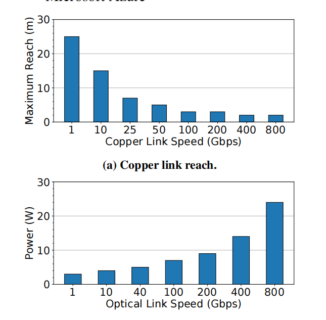
This trade-off is not static; it is worsening with each successive generation of network hardware. As link speeds escalate to 400 Gbps, 800 Gbps, and beyond, the physical limitations of these technologies become more pronounced. The reach of copper links continues to shrink, while the power consumption of optical links grows unabated. This trend suggests an impending “networking wall,” a scenario where the interconnects themselves become the primary bottleneck to scaling data center performance and efficiency, leading to spiraling deployment costs, unsustainable power demands, and compromised reliability.
The “Networking Wall”: Scaling Bottlenecks of the Narrow-and-Fast (NaF) Architecture
The root cause of this escalating crisis is the shared reliance of both copper and optical technologies on a “Narrow-and-Fast” (NaF) architecture. This design paradigm achieves high aggregate bandwidth by using a small number of serial channels, each operating at extremely high speeds (e.g., an 800 Gbps link composed of eight 100 Gbps channels). For copper, higher data rates necessitate higher modulation frequencies, which suffer from greater signal attenuation due to physical phenomena like the skin effect and dielectric loss. This results in a near-linear relationship where signal loss increases with frequency, effectively halving the achievable reach with each new generation. For optical links, the NaF approach is inherently power-inefficient. Pushing channel speeds to 100 Gbps and beyond requires a cascade of power-hungry electronic components, including complex digital signal processors (DSPs), high-speed analog-to-digital and digital-to-analog converters (ADCs/DACs), and clock-and-data recovery (CDR) circuits. Furthermore, operating optical components like lasers and modulators at these speeds reduces system margins and tolerance to noise, increasing failure rates.
The recently announced NVIDIA NVL72 pod serves as a stark, real-world illustration of this dilemma. To interconnect 72 high-power GPUs, NVIDIA faced a choice: using optics would have added a prohibitive 20 kW of power consumption per rack, while typical optical failure rates would have caused a disruptive link failure every 6-12 hours in a large-scale cluster. Consequently, they opted for copper, but its short reach forced an extremely dense design, packing all 72 GPUs into a single 120 kW rack that requires complex and costly liquid cooling solutions.The problem is not merely technical; it has profound economic consequences. The high power consumption of optics directly inflates operational expenditure (OpEx), while poor reliability increases maintenance costs and, more critically, leads to costly downtime for large, synchronous AI workloads.
MOSAIC’s Thesis: The Wide-and-Slow (WaS) Paradigm
In response to this challenge, the paper introduces MOSAIC, a novel optical link technology founded on a fundamentally different architectural principle: “Wide-and-Slow” (WaS). Instead of a few high-speed channels, MOSAIC employs hundreds of parallel, low-speed optical channels. This is not an incremental improvement but a paradigm shift that aims to break the existing trade-off entirely. The central claims of the MOSAIC project are to deliver a link technology that achieves 10x the reach of copper (up to 50 m), reduces power consumption by up to 68% compared to contemporary optical links, and offers 100x higher reliability, all while maintaining backward compatibility with existing network infrastructure.
| Feature | Copper Links | Traditional Optical Links | MOSAIC |
|---|---|---|---|
| Architecture | Narrow-and-Fast (NaF) | Narrow-and-Fast (NaF) | Wide-and-Slow (WaS) |
| Reach | < 2 m (shrinking) | Tens of meters | Up to 50 m |
| Power | Very Low (Passive) | High (growing) | Low (up to 68% savings) |
| Reliability | Very High (<10 FIT) | Low (100s of FIT) | Very High (~10 FIT) |
| Key Bottleneck | Signal Attenuation | Power-Hungry DSP/Lasers | Dispersion |
The MOSAIC Architecture: A Deep Dive into the Wide-and-Slow Paradigm
The practicality and effectiveness of the WaS architecture depend on a synergistic combination of novel optoelectronic components, innovative optical design, and a radically simplified electronic backend. This section deconstructs the key building blocks of the MOSAIC design.
Core Optoelectronic Components
MicroLEDs and CMOS Sensors: The Engine of WaS
The cornerstone of the MOSAIC architecture is the use of directly modulated microLEDs as the optical source, a departure from the power-hungry lasers used in traditional optical links. Originally developed for the consumer display industry, microLEDs possess a unique set of characteristics that make them ideal for a WaS design. They operate at extremely low power levels—on the order of hundreds of microwatts (µW) per channel, compared to tens or hundreds of milliwatts (mW) for lasers. Their small size allows them to be fabricated in dense 2D arrays, with over 400 channels fitting within a 1 mm2 die. Furthermore, their simpler physical structure, which relies on spontaneous rather than stimulated emission, makes them intrinsically more reliable and less sensitive to temperature variations than lasers. This approach represents a strategic leveraging of mature, high-volume consumer technology to disrupt the specialized, lower-volume data center optics market, thereby piggybacking on billions of dollars of external R&D to drive down costs and diversify the supply chain.
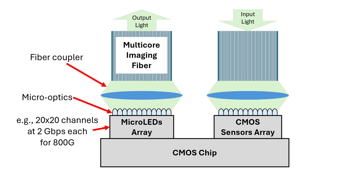
However, microLEDs introduce two primary challenges. First, they are Lambertian emitters, meaning they emit light in a wide, uncollimated beam, which complicates coupling into a fiber and can cause crosstalk. Second, they have a much broader emission spectrum (tens of nanometers) compared to lasers, which exacerbates chromatic dispersion in the fiber. MOSAIC addresses these challenges through a combination of custom optics and a simplified electronic backend. On the receiver side, the use of visible light allows for low-cost CMOS sensors, similar to those in smartphone cameras, which can be monolithically integrated with the receiver electronics for further cost and power savings.
Custom Micro-Optics: Taming the Light
To solve the problem of inefficient light coupling and potential crosstalk from the microLEDs’ wide beam, MOSAIC employs a novel custom lens design based on the principle of Total Internal Reflection (TIR). Initial experiments with standard micro-lens arrays (MLAs) proved insufficient to capture the wide-angle light. The custom TIR lens, in contrast, features a two-component design that effectively traps and collimates the light, resulting in more than double the coupling efficiency of a standard MLA. This collimation is critical not only for maximizing the power delivered to the fiber but also for mitigating a key physical impairment. As clarified during the presentation’s Q&A session, the wide emission angle of microLEDs is a primary cause of modal dispersion, where different light paths (modes) travel at different speeds. By narrowing the beam into a cone of approximately ±12∘, the TIR lens directly combats modal dispersion by limiting the range of modes launched into the fiber.
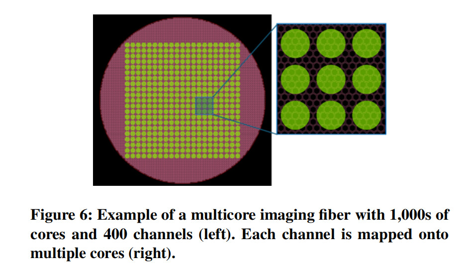
Multicore Imaging Fiber: The WaS Conduit
Managing hundreds of individual fibers would be prohibitively complex and costly. MOSAIC overcomes this by using a single multicore imaging fiber, another technology repurposed from a high-volume external market (medical endoscopy). These fibers contain thousands of individual cores within a single strand, providing a practical and cost-effective conduit for a massive number of parallel channels. This approach greatly simplifies packaging and deployment. To further reduce manufacturing complexity, MOSAIC’s design maps a single microLED onto multiple fiber cores, which significantly relaxes alignment tolerances. Because the entire fiber is fabricated in a single process, the transmission characteristics and lengths of all cores are highly uniform, resulting in negligible channel-to-channel skew, a critical property for maintaining synchronization across the wide parallel bus.
The Power of Simplified Electronics
The most significant advantage of the WaS architecture’s low per-channel speed (e.g., 2 Gbps in the prototype) is the radical simplification of the electronic backend. This is where the majority of power savings are realized. High-speed NaF links require complex DSPs to compensate for signal impairments and power-hungry ADCs/DACs for multi-level signaling schemes like 4-level Pulse Amplitude Modulation (PAM-4). MOSAIC eliminates this entire digital backend. It relies on a simple, robust ON-OFF (Non-Return-to-Zero, NRZ) signaling scheme, which has much less stringent signal-to-noise ratio (SNR) requirements. Any remaining transmission impairments, primarily chromatic dispersion, are handled by a low-power analog equalization circuit. This co-design, where the custom optics mitigate modal dispersion and the simple analog electronics handle chromatic dispersion, is a key element of MOSAIC’s efficiency.
System-Level Enhancements via Channel Overprovisioning
The MOSAIC architecture does more than just improve the physical link’s core metrics; it enables a new class of system-level features by making channel redundancy economically feasible. The low marginal cost of adding extra microLED channels in a WaS design allows for overprovisioning, which is leveraged to create an intelligent and resilient interconnect subsystem.
Achieving Copper-Class Reliability
A primary claim of MOSAIC is its ability to match the high reliability of passive copper cables. This is achieved through an innovative two-layer fault tolerance mechanism. The first layer consists of a lightweight, low-latency error correction code (ECC), such as Hamming coding, applied across blocks of data channels. This ECC can detect and correct a single-channel failure in real-time, masking the error from the higher layers of the network stack without interrupting data flow or exceeding the pre-FEC Bit Error Rate (BER) threshold. The second layer involves maintaining a set of “hot spare” channels. When the ECC detects a persistent failure, the system seamlessly switches the data stream from the failed channel to a spare one. This combination provides near-zero downtime upon channel failure. For an 800 Gbps link requiring 400 data channels, this level of protection can be achieved with approximately 60 additional parity and spare channels, representing a modest 15% overhead. This fundamentally transforms the link from a passive wire into a self-healing system capable of absorbing multiple component failures without service interruption, a significant shift in the network abstraction layer.
Optimizing for Power and Simplicity
Channel overprovisioning is also used to reduce power consumption and complexity further. In one such optimization, a spare channel is dedicated to forwarding the clock signal directly from the transmitter to the receiver. This simple yet effective technique eliminates the need for a power-hungry and area-intensive Clock-and-Data Recovery (CDR) circuit at the receiver, which is a standard and costly component in all high-speed serial links.
Furthermore, clock forwarding enables power proportionality, a feature where the link’s power consumption scales with its actual utilization. Because the receiver’s clock is always present, the data channels do not need to transmit continuously to maintain synchronization. During idle periods, MOSAIC can progressively deactivate data channels. As outgoing packets fill a transmit queue, channels are reactivated as needed. This dynamic scaling aligns power consumption with real-time traffic load, offering substantial energy savings, particularly for the asymmetric, bursty traffic patterns common in workloads like AI inference.
Power Consumption Analysis
The cumulative effect of these architectural choices results in a dramatic reduction in overall power consumption. An analysis comparing a projected 800 Gbps MOSAIC module to a contemporary 800 Gbps optical AOC shows that MOSAIC reduces power per end of the link from 9.8-12 W to 3.1-5.3 W, a saving of 56-68%. The most significant savings come from the elimination of the digital backend (a reduction from 3.5 W to 0.4 W) and the lower power of the analog frontend and microLED emitters (a reduction from 4.7 W to 1.2 W). This substantial power efficiency directly addresses one of the primary scaling challenges facing modern data centers.
Prototype and Evaluation: From Concept to Reality
To validate its design principles, the MOSAIC project developed an end-to-end prototype and conducted extensive simulations to project the performance of a production-grade module. This two-pronged evaluation strategy effectively de-risks the technology by first proving the fundamental viability of the architecture and then providing a credible engineering path to a commercially competitive product.
The 100-Channel End-to-End Prototype
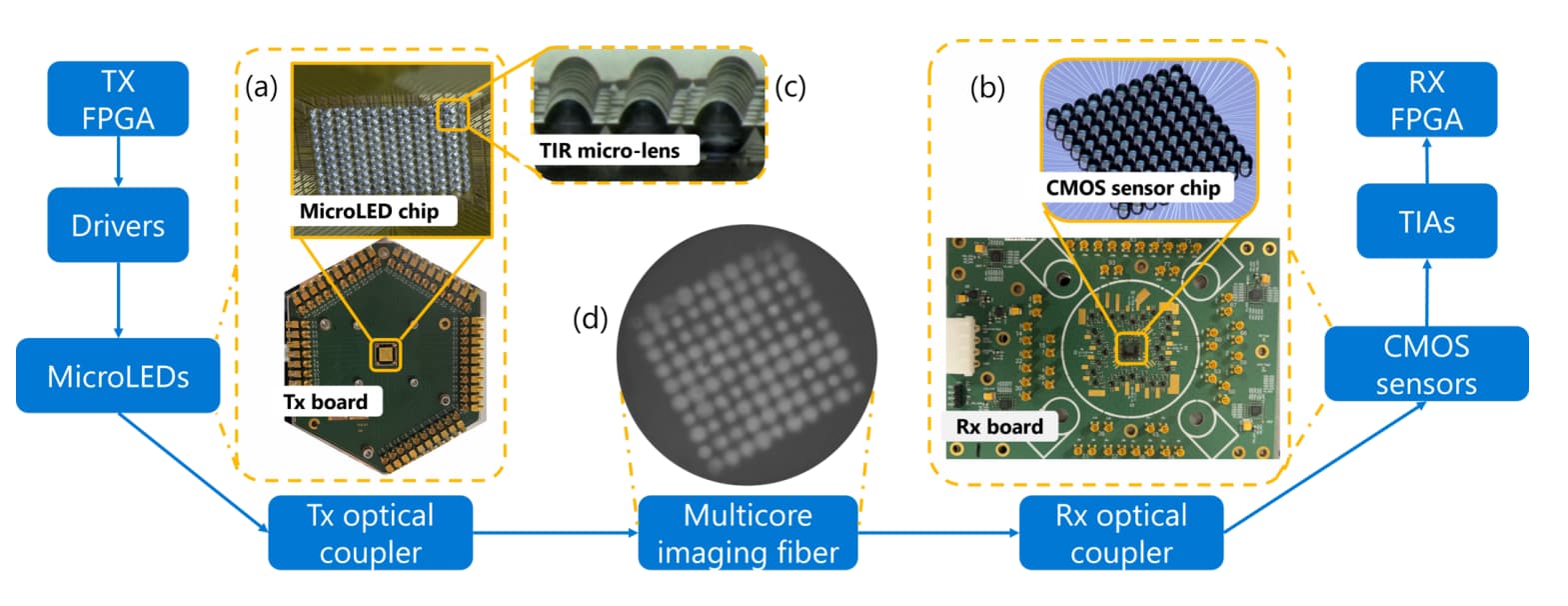
The physical prototype consisted of 100 channels, built using bespoke 10×10 microLED and CMOS sensor arrays wire-bonded to printed circuit boards (PCBs). FPGAs were used to emulate the simplified electronic backend, generating and receiving data streams. The custom TIR micro-lenses were fabricated and mounted on the arrays, and a combination of discrete lenses was used to couple the light into and out of a multicore imaging fiber. This setup, while constrained by the limitations of prototyping (e.g., bulky discrete components and signal integrity challenges from wire-bonding), was sufficient to validate the core concepts of the MOSAIC design.
Experimental Results and Key Findings
Experiments conducted with the prototype successfully demonstrated the feasibility of the WaS architecture.
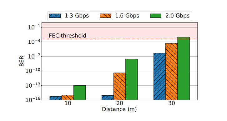
- BER Performance: In tests using 25 channels simultaneously, all channels achieved a BER well below the industry-standard FEC threshold of 2×10⁻⁴. The median BER was measured at less than 2×10⁻⁸, confirming that even with non-ideal components, the link quality is more than sufficient for data center applications.
- Speed vs. Distance: The prototype successfully transmitted data at 2 Gbps over a 20-meter fiber and at 1.6 Gbps over a 30-meter fiber, all while maintaining a BER below the FEC threshold. This result, achieved despite the prototype’s known limitations, validates the underlying physics of the approach.
- Fault Tolerance Demonstration: The two-layer reliability mechanism was tested on a live 10 Gbps Ethernet link. In this experiment, two channels were artificially failed in real time. The combination of ECC and hotswapping successfully masked and recovered from both failures with no impact on the link’s reported BER and no service interruption, providing a powerful demonstration of the system’s resilience.
Scaling to Production: Simulation and Analysis
Building on the validated foundation of the prototype, simulations were used to project the performance of a production-grade 800 Gbps pluggable module that would leverage standard integration techniques like vertically bonded chips and custom fiber couplers.
- Distance and Speed Scalability: These simulations indicate that a production module could achieve 2 Gbps per channel over distances up to 50 meters, or scale to over 8 Gbps per channel for shorter links up to 10 meters, all with a comfortable BER margin.
- Reliability at Scale (FIT Analysis): Large-scale reliability simulations analyzed the link’s overall Failure In Time (FIT) rate. The results showed that with no redundancy, the FIT rate would be comparable to or worse than traditional optics. However, adding just 5% redundant channels (20 spares for a 400-channel link) was sufficient to reduce the FIT rate by an order of magnitude, bringing it into the range of highly reliable copper cables.
- Optical Fidelity: To confirm the optical design scales to hundreds of channels, commercial ray-tracing software was used to model a 460-channel system. The simulations verified high coupling efficiency and showed that the light beams from individual channels remained clearly separated with virtually zero crosstalk, validating the optical design’s scalability.
Presentation Q&A Session Analysis
The Q&A session following the paper’s presentation provided additional context and explored the future implications of the MOSAIC technology, revealing nuances not fully detailed in the written text.
Full Q&A Transcript
Moderator: Thank you. Very nice talk, very inspiring talk. So, questions?
Questioner 1: Thanks so much for the talk. I actually have a little bit more detailed question. So, in your paper, you focus on 20 to 30 meter links and you basically… Can you hear? Yeah, okay. So, in your paper, you basically focus on 20 to 30-meter links, right? And you focus on chromatic dispersion as the main culprit. Most of the published LEDs focus on shorter links due to modal dispersion. Can you comment on how the modal and chromatic dispersion compare with your links? And if you did something special other than obviously the lens to combat the modal dispersion and the EQ use, the equalization?
Presenter: Yeah, it’s a great question, actually. So, both dispersions are important to us. So, for example, as you know, the… Even though we say it’s a single color, it’s actually many, many shades of different colors. So, different colors will be propagated at different speeds, that is limiting on the chromatic dispersion. And also because the micro LEDs, as I said, the light beams go at a wider angle. So, different angles will also propagate at different speeds, which is also kind of causing the modal dispersion. So, for us, especially for the long transmission distance that we are targeting, both are extremely important for us. We have to tackle both.
Questioner 1: Okay. So, in your paper, you only mentioned chromatic. So, you are actually seeing both dispersion? Yeah. And any special EQs you used? Any special?
Presenter: Equalization?
Questioner 1: Equalization?
Presenter: No, as I said, because the speed or the rate that we are running at is really, really low. So, any standard equalization techniques we’re using in the electric domain can be implemented here. And then it’s quite efficient to be able to implement them at such a low rate in general.
Questioner 1: If I may, one more question on the fiber. Can you comment on the material NA and the field factor for the imaging fiber?
Presenter: Sorry, the material and?
Questioner 1: NA, the optical.
Presenter: That’s a bit of a specific question, but I can say that, again, the fiber for us, the important part is that we need a low-cost fiber that will be able to support hundreds of channels. We are open to many different types of technologies.
Questioner 1: I’ll come find you.
Presenter: Thank you. Thank you.
Questioner 2: Hi, thank you. That was very interesting. So, simple question. How many speeds that you have today that are 200 gigabits per second? And if I wanted to replace that with one of these micro LED arrays, how many LEDs would I require?.. How many? How many would I require to get the same bandwidth? I’m trying to do a calculation based on the beachfront to the area.
Presenter: Yeah. So, as you see, for example, when the 800 GB, we were using 400 channels. Each of which is running at two gig for the next generation. Obviously, there are different ways to, for example, further scale the speed. One way you can think is probably we can increase the line rate for each micro LED to run a bit faster. And the other way to introduce in more channels. So, I think the combination of these two will allow us to really scale…
Questioner 2: Okay, let me step back. The essential problem today is how to get the maximum I/O out of a chip, because you are bound by the beachfront of the chip, right? And so if you’re trying not to be bound by the beachfront, but you want to have the area on top so that you scale by the square of the size of the chip, not by linear dimensions… I’m trying to see if I can project ahead and would like to get your best guess on that.
Presenter: Yeah, it’s going to be hard to predict, because there are still a lot of challenges that need to be solved on the packing side, for example, the thermal issues and all these kinds of things. But that’s definitely one of the directions to go, because for us, by nature, it’s a 2D array, so it’s quite easy to be able to fully utilize an area rather than just a shoreline… But to your point, fundamentally, we do want to, well, it will be great to be able to see them being integrated. But again, the packaging, the whole stack needs to be fully optimized coherently. Thank you.
Questioner 3: I loved your talk. Super. Really exciting… I have a different question. And this is about what you think the consequences are. What are you thinking in terms of the optical switch design? Because now it’s actually got to switch a whole bundle… Or do you think that the lower power means you actually don’t need an optical switch, you would actually convert back to the electronic domain?
Presenter: It’s a great insight. I would say it can be both. It depends on the final power… We have actually developed a couple of technologies to make this compatible with an optical circuit switch and a relatively high radix as well. And on the other hand, there could be another design if, as you said, the efficiency of the link transmitting data has become so low that we may not need it. So yeah, I would say both of your insights are something that we are looking at.
Analysis of Key Discussion Points
The Q&A session provided several crucial clarifications and forward-looking perspectives:
- Dispersion Deep Dive: The first question prompted a key clarification regarding signal impairments. While the paper focuses on chromatic dispersion (caused by the microLED’s broad spectrum), the presenter confirmed that modal dispersion (caused by the wide emission angle) is equally critical for the targeted link distances. This reveals a more nuanced co-design: the TIR micro-optics are not just for improving coupling efficiency but are a primary tool for combating modal dispersion, while the simple analog equalizer is tasked with handling the remaining chromatic dispersion.
- Scaling and Integration: Beyond the “Shoreline”: The most profound exchange centered on the future of chip-level I/O. The questioner astutely framed the current limitation of high-performance chips as being bound by their perimeter, or “beachfront.” They proposed that MOSAIC’s 2D array nature could enable a shift from this linear constraint to scaling I/O with the chip’s surface area. The presenter confirmed this is a key future direction, envisioning a scenario where a MOSAIC array could be integrated directly on top of a GPU or switch ASIC. This concept elevates MOSAIC from a better interconnect to a foundational technology for next-generation computing. It suggests a path to bypass the package pin bottleneck entirely, enabling true chiplet ecosystems where processors, memory, and accelerators are interconnected with massive bandwidth over meter-scale distances—a revolutionary leap beyond today’s on-package interconnects.
- Implications for Optical Switching: The final question explored MOSAIC’s relationship with all-optical networking. The presenter’s response indicated two potential futures. On one hand, MOSAIC’s bundled nature could be made compatible with optical circuit switches. On the other hand, MOSAIC could become so power-efficient that traditional electrical switching (O-E-O) remains economically superior to all-optical solutions for many applications. This highlights an important strategic question for the future of data center network design: does MOSAIC complement or compete with the vision of an all-optical data center?.
Personal Thoughts and Critical Analysis
The MOSAIC project presents a compelling and well-engineered solution to one of the most pressing challenges in data center scaling. Its core strength lies in its elegant, first-principles approach to breaking the long-standing trade-off between reach, power, and reliability that has defined network interconnects for decades.
Strengths and Contributions
MOSAIC’s primary contribution is the practical realization of the Wide-and-Slow architecture for optical links. The clever repurposing of mature, high-volume technologies from the consumer display and medical industries—microLEDs and imaging fibers—is a brilliant strategic move to drive down cost and leverage external R&D ecosystems. The design is comprehensive, extending beyond the physical layer to incorporate system-level features like fault tolerance and power proportionality that are uniquely enabled by the WaS paradigm. Finally, its commitment to backward compatibility as a “drop-in replacement” for existing QSFP/OSFP modules provides a practical and non-disruptive path to adoption.
Potential Challenges and Limitations
Despite its technical promise, MOSAIC faces significant non-technical hurdles on its path to widespread adoption. The most substantial challenge is logistical: building a robust manufacturing and supply chain ecosystem for data-center-grade microLED arrays, custom TIR lenses, and imaging fibers. This will require significant industry investment, collaboration, and standardization. On the engineering front, the challenges of packaging hundreds of optical channels into a compact, thermally stable, and high-yield pluggable module are non-trivial. While simulations are highly promising, real-world, long-term reliability data for these novel components operating 24/7 in harsh data center environments will be necessary to fully validate the technology’s impressive FIT rate claims.
Broader Impact: A Catalyst for the Next Computing Epoch
Ultimately, the vision for MOSAIC extends far beyond being a better cable. As articulated in the paper’s discussion section and reinforced in the Q&A, MOSAIC is positioned as a potential enabler for the next generation of distributed computing systems. By providing an interconnect with the power and reliability of copper but the reach of optics, it could fundamentally reshape data center network topologies, making direct-connect server architectures and the elimination of Top-of-Rack switches practical. It stands as a promising candidate to finally unlock the long-sought-after goal of resource disaggregation, enabling memory and GPUs to be pooled and composed dynamically. Most profoundly, as hinted in the discussion of area-based I/O, MOSAIC could revolutionize the design of processors themselves, breaking the I/O bottleneck that currently constrains high-performance computing. If it can overcome the challenges of commercialization, MOSAIC has the potential to be a key foundational technology driving the next era of innovation in computing architecture.